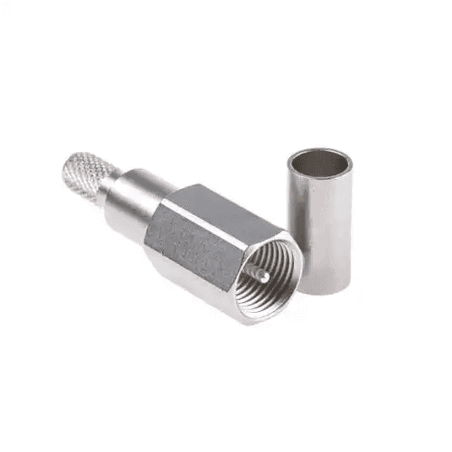
A connector contact may be only a few millimeters in diameter, but its manufacturing requirements extend far beyond the dimensions of a simple turned component. The contact must fit within its insulator, engage correctly with the mating interface, carry electrical current or signals, and maintain mechanical and electrical performance throughout its intended service life.
A small dimensional error can become significant when multiple requirements interact. A pin machined to the correct diameter before plating may exceed its final tolerance after nickel and gold deposition. A tiny burr at the entrance of a socket can interfere with insertion, while an incorrectly positioned shoulder may prevent the contact from seating properly in the connector housing.
Precision connector contact machining requires coordinated control of material selection, machining tolerances, surface finishing, plating thickness, and final inspection.
This guide explains how to design and manufacture CNC-machined connector pins, sockets, terminals, and contact bodies. It focuses on practical engineering decisions, including the selection of conductive copper alloys, machining process capabilities, plating allowances, and the dimensional requirements that should appear on a production drawing.
What Makes Connector Contact Machining Different?
Machined connector contacts are commonly produced from conductive metal bar stock using CNC turning, Swiss-type turning, or mill-turn machining. They may incorporate stepped diameters, grooves, internal bores, retention shoulders, solder cups, crimp barrels, and other functional features.
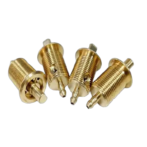
Unlike many conventional turned parts, connector contacts have both mechanical and electrical requirements. A shaft is primarily designed to support or transmit mechanical loads, while a connector contact must establish and maintain a reliable electrical interface.
The required manufacturing accuracy depends on the specific contact design.
Fixed Pins and Power Contacts
Fixed electrical contacts generally depend on correct diameter, engagement length, alignment, and the performance of a separate mating spring or socket element.
Power contacts must also account for current rating, contact resistance, temperature rise, and the mechanical retention of the contact within its insulating housing.
For these components, machining accuracy is important, but material conductivity and the reliability of the complete electrical connection are equally significant.
Socket Contacts and Spring Interfaces
Socket contacts may contain internal bores, slotted contact fingers, or separate spring elements. Their manufacturing challenges include internal geometry, wall thickness, burr control, and the effects of plating on mating clearances.
The contact force often comes from a separate spring mechanism or an appropriately designed spring alloy. A rigid, free-machining brass socket should not automatically be treated as having the fatigue resistance of a purpose-designed spring contact.
RF and Coaxial Connector Contacts
RF connector center contacts may require particularly careful control of diameter, axial position, alignment, and surface condition.
At high frequencies, connector geometry and the surrounding dielectric structure influence impedance and RF performance. An accurately machined center pin alone does not establish the electrical performance of the assembled connector.
For RF applications, dimensional requirements should be established from the connector design and verified through appropriate assembly-level testing.
Choosing the Right CNC Machining Process
The most suitable machining method depends on component diameter, length-to-diameter ratio, feature complexity, material, production quantity, and inspection requirements.
Related service: mill-turn machining
Related service: CNC turning services
Swiss-Type CNC Turning
Swiss-type turning is particularly useful for small-diameter, slender components because the guide bushing supports the bar stock close to the cutting area.
This configuration can help reduce workpiece deflection during machining, especially for long pins, narrow contact tails, and other features that are difficult to support in conventional turning.
Typical applications include miniature connector pins, stepped electrical contacts, precision terminal bodies, and components with multiple small diameters.
However, Swiss turning is not automatically the best process for every contact. Bar straightness, material condition, guide-bushing requirements, setup cost, and part geometry all influence the result.
CNC Turning and Mill-Turn Machining
Conventional CNC turning is well suited to relatively short, rigid contacts containing cylindrical features such as diameters, grooves, threads, and internal bores.
Mill-turn machining becomes attractive when the contact also requires cross-holes, flats, milled slots, or indexed features.
For example, a connector contact containing a turned mating diameter, an axial solder cup, and two cross-holes may benefit from being manufactured in a single mill-turn setup. Reducing workpiece transfers can help control the positional relationship between features and simplify production.
| Contact geometry | Suitable process | Main manufacturing concern |
|---|---|---|
| Long, slender contact pin | Swiss turning | Deflection, straightness, small diameters |
| Short stepped pin | CNC turning | Shoulder location, diameters |
| Socket with axial bore | CNC turning or Swiss turning | Internal burrs, bore dimensions |
| Contact with flats and cross-holes | Mill-turn machining | Feature alignment, burr formation |
| Contact with deep solder cup | CNC turning, drilling, or mill-turn | Bore depth, concentricity, cleanliness |
| Prototype contact with complex geometry | Selected multi-process approach | Setup cost, tolerance transfer |
The objective is to manufacture the functional features accurately and repeatably, not simply to use the most sophisticated machine available.
Connector Contact Materials: C110 vs. C145 vs. C360
Material selection affects conductivity, mechanical strength, machining efficiency, plating compatibility, joining behavior, and cost.
Related service: CNC machining materials
Three common candidates for machined electrical components are C11000 electrolytic tough pitch copper, C14500 tellurium copper, and C36000 free-cutting brass. They are not direct substitutes because their electrical and machining properties differ substantially.
Material Comparison
| Material | Typical conductivity | Relative machinability rating | Potential use |
|---|---|---|---|
| C11000 ETP Copper | ~100–101% IACS | ~20 | High-conductivity contacts, terminals |
| C14500 Tellurium Copper | ~93% IACS | ~85 | Precision turned conductive contacts |
| C36000 Free-Cutting Brass | ~26% IACS | 100 reference | Contact bodies and cost-sensitive turned components |
Material reference data: C11000, C14500, C36000
Values are indicative material reference figures, not finished-part performance guarantees. Conductivity, strength, and other properties depend on alloy specifications and material condition. Machinability ratings are relative reference values.
C11000: When Conductivity Is the Priority
C11000 offers high electrical conductivity and is useful where current-carrying performance is a dominant requirement.
Its main difficulty in precision turning is its relatively ductile behavior. The material can generate long chips, smear around cutting edges, and develop burrs that require careful control.
For a simple power terminal with generous geometry, these manufacturing challenges may be acceptable. For a miniature contact containing multiple small grooves, thin walls, and cross-holes, additional machining and deburring effort may increase production cost.
C14500: Balancing Conductivity and Machinability
C14500 tellurium copper is a strong candidate for precision machined electrical contacts because it combines relatively high conductivity with improved chip-breaking behavior.
Compared with C11000, C14500 can simplify the machining of small diameters, shoulders, grooves, threads, and other detailed features.
This makes it attractive for connector components in which the benefits of improved machining productivity justify the material selection.
However, tellurium copper is not the preferred choice for every joining method or operating environment. Material form, temper, joining requirements, and special service conditions should be reviewed before specifying it.
C36000: Machinability and Cost Efficiency
C36000 brass is widely used for precision turned components because of its excellent machinability.
It is suitable for connector components where the design permits lower electrical conductivity than copper grades. Its chip-breaking characteristics can support efficient machining of intricate features.
A key consideration is its lead content. C36000 typically contains approximately 2.5–3.0% lead, so applicable material restrictions, product compliance requirements, and customer specifications must be evaluated. It should not be described as universally RoHS compliant without verifying the relevant requirements and any applicable exemptions.
What About Phosphor Bronze and Beryllium Copper?
Not every connector contact should be made from free-machining copper or brass.
When the component must repeatedly flex to maintain electrical contact force, spring behavior becomes a major selection criterion.
Phosphor bronze is commonly used for contact springs and stamped terminals because it offers useful spring properties and fatigue performance.
Beryllium copper, such as C17200, may be considered for demanding spring contacts where high strength and elastic performance are required after appropriate processing. Machining, heat treatment, occupational safety controls, and regulatory requirements need specific consideration.
The design must distinguish between the conductive contact body and the element responsible for generating contact force. In some connectors, these functions are performed by separate components using different materials.
Realistic Machining Tolerances for Connector Contacts
A connector drawing should not apply the same precision requirement to every feature. The mating diameter, contact retention shoulder, solder cup, and nonfunctional exterior surfaces have different roles and therefore may justify different tolerance limits.
The most useful approach is to identify the features that determine assembly and electrical performance, then control those dimensions individually.
Which Features Need Tight Tolerances?
| Feature | Why it matters | Recommended control |
|---|---|---|
| Mating pin diameter | Fit and engagement with mating socket | Finished diameter and surface condition |
| Contact shoulder | Axial positioning in insulator | Shoulder-to-datum distance |
| Retention diameter | Press fit or retention mechanism | Diameter, geometry, surface condition |
| Solder cup ID | Wire insertion and soldering | Bore diameter, depth, cleanliness |
| Crimp barrel ID | Conductor fit and crimp quality | Size and validated crimp geometry |
| Contact alignment | Mating behavior | Runout or position relative to functional datum |
| Contact surface | Wear and electrical performance | Roughness, plating, defect criteria |
| Plating boundary | Coated functional area | Defined start/end points and masking |
For preliminary manufacturability discussions, ±0.02 mm may be considered for certain small turned features, with ±0.01 mm potentially feasible on selected rigid, accessible geometries.
These are not universal connector machining tolerances. The achievable result depends on the component’s diameter, geometry, material, tool access, workholding, production quantity, and inspection method.
A tolerance of ±0.005 mm, for example, may be technically achievable on a selected feature, but it needs process-specific evaluation. Applying that tolerance to every diameter and shoulder would unnecessarily complicate many designs.
Dimensional Accuracy Is Not the Same as Runout
Consider a connector pin with two stepped diameters. Both may meet their size tolerances, while their rotational axes are not sufficiently aligned.
This can cause difficulty during mating, particularly where the connector has limited radial clearance.
For rotational contacts, circular runout, total runout, or positional controls may be appropriate depending on the functional requirement.
The datum should normally correspond to the feature that establishes the contact’s position in the assembled connector.
Using the largest diameter as a datum without considering how the contact is actually located may produce a drawing that is difficult to inspect or does not control the intended function.
Surface Roughness and Contact Reliability
Surface roughness influences mechanical engagement, wear, and the condition of the substrate beneath a plated contact surface.
A turned finish around Ra 0.8–1.6 μm can be a reasonable starting point for discussing certain noncritical locating or contact-related surfaces, but critical mating zones may require a different specification.
The appropriate requirement depends on the mating geometry, contact force, plating system, wiping action, and service environment.
An important distinction is that Ra alone cannot establish whether a connector contact surface is acceptable. A single scratch, dent, embedded particle, or plating defect can cause problems even when an average roughness measurement is within its specified limit.
Drawings should define functional surface requirements separately from general cosmetic expectations.
How Gold and Nickel Plating Affect Connector Dimensions
Plating allowance is one of the most important—and most frequently misunderstood—parts of connector contact manufacturing.
Related service: surface finishing options
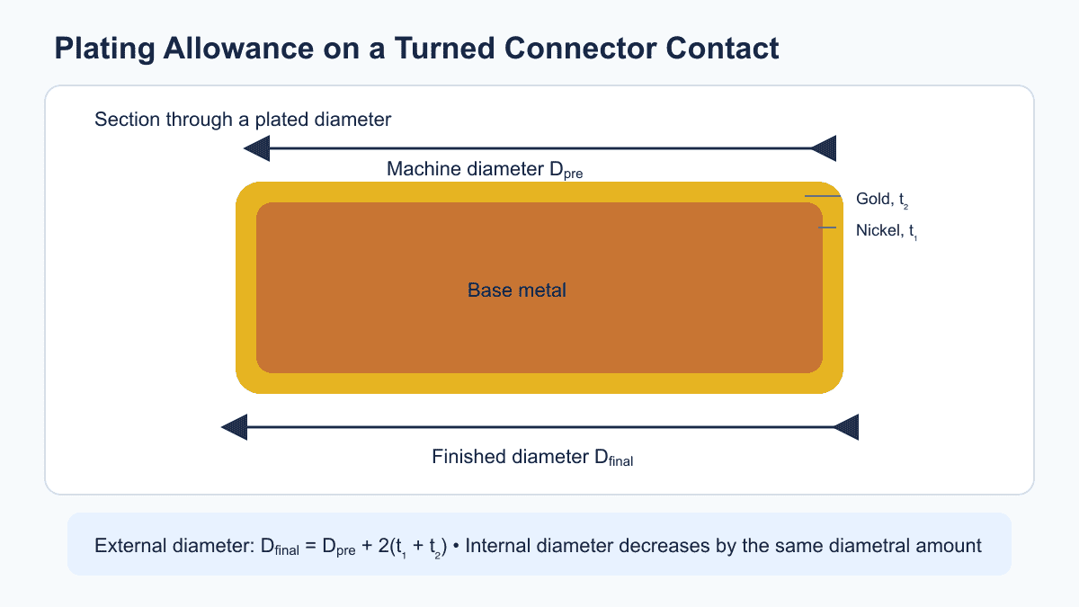
Electrical contacts are often machined before receiving nickel, gold, silver, tin, or another specified coating. Because plating adds material to exposed surfaces, the finished dimensions may differ from the dimensions measured immediately after machining.
For a precision pin or socket, even a few micrometers of coating can consume a significant portion of the available tolerance.
Why Nickel and Gold Are Often Used Together
Gold is valued in connector applications for corrosion resistance and low, relatively stable contact resistance when the coating is properly specified and applied.
Nickel is commonly used beneath gold to provide a barrier layer and support the performance of the overall coating system.
The selected coating thickness, gold composition or hardness classification, underplate, and acceptance tests depend on the application. ASTM B488 addresses electrodeposited gold coatings for engineering uses, including specified coating properties and verification requirements.
A connector designed for occasional mating in a controlled environment may have different coating requirements from a frequently mated industrial connector exposed to vibration, humidity, and contamination.
The plating stack should be chosen according to the complete electrical and mechanical design, rather than treating gold thickness as a universal quality indicator.
How Plating Changes External and Internal Diameters
Nickel and gold are deposited on exposed surfaces. On a uniformly plated outside diameter, the coating adds thickness on both sides.
For a uniformly plated cylindrical outside diameter:
D_final = D_machined + 2 × (t_Ni + t_Au)
For a uniformly plated internal bore:
D_final = D_machined − 2 × (t_Ni + t_Au)
Use the same unit for the diameter and coating thickness in these equations: 1 μm = 0.001 mm.
Where:
- D_final is the diameter after plating.
- D_machined is the diameter before plating.
- t_Ni is nickel thickness on one surface.
- t_Au is gold thickness on one surface.
These equations describe ideal uniform deposition. Actual coating thickness varies according to component geometry, current distribution, plating process, masking, and measurement location.
Worked Example: Gold-Plated Connector Pin
Consider a connector pin with the following hypothetical requirements:
| Parameter | Specified value |
|---|---|
| Finished mating diameter | Ø2.000 ±0.010 mm |
| Nickel underplate | 2.0–3.0 μm per surface |
| Gold coating | 0.8–1.2 μm per surface |
| Coating coverage | Entire mating diameter |
The minimum combined coating thickness per surface is:
2.0 + 0.8 = 2.8 μm per surface
The maximum combined thickness is:
3.0 + 1.2 = 4.2 μm per surface
Because both sides of the pin receive coating, the total diameter increase is:
Diameter increase = 0.0056–0.0084 mm
This means that a pin machined to exactly Ø2.000 mm would finish approximately between Ø2.0056 and Ø2.0084 mm under the assumed uniform-coating model.
That may fit within the required final tolerance, but it leaves very little room for positive machining variation.
Calculating the Worst-Case Pre-Plating Window
Using the example above, the acceptable post-plating diameter is 1.990–2.010 mm.
To guarantee that range for all coating thicknesses within the stated limits, the machined diameter would have to satisfy:
D_machined ≥ 1.990 − 0.0056 = 1.9844 mm
and
D_machined ≤ 2.010 − 0.0084 = 2.0016 mm
Therefore, the theoretical acceptable pre-plating range is:
Theoretical pre-plating diameter window: 1.9844–2.0016 mm
This calculation is more useful than simply subtracting a nominal plating thickness from the finished diameter.
However, it is only a starting point. Real coating variation may be correlated with part geometry and plating position, and local coating thickness may differ from the assumed values.
If the theoretical pre-plating window is narrower than the achievable machining process, or if actual plating variation exceeds the available allowance, the manufacturing plan needs to change.
Possible options include improved plating control, selective coating, revised dimensional requirements, or other approved process adjustments.
Interactive Plating Allowance Calculator
Assumes uniform coating and the stated worst-case thickness limits. Actual coating distribution, machining capability and measurement uncertainty must be verified. All coating inputs are thicknesses per surface.
Internal Socket Diameters Need Special Attention
Plating an internal socket is more difficult to model than plating a simple external pin.
A cylindrical bore becomes smaller as coating builds on its internal surfaces. However, the coating may not distribute evenly along the bore, especially in deep recesses or narrow blind holes.
Electrical current distribution, solution access, surface geometry, and plating method can affect local deposition.
For example, a socket may receive adequate nickel and gold thickness near its entrance while the coating farther inside differs from the specified target.
A diameter measurement at the socket opening does not necessarily verify the condition deeper within the bore.
Engineers should therefore define which internal surfaces are electrically functional, where coating thickness must be measured, and whether the design requires specialized plating process validation.
Selective Plating vs. Full-Body Plating
Not every surface on a connector contact needs the same coating.
A component may require a wear-resistant gold finish on its mating zone, while the termination region uses a different finish for soldering or crimping.
Selective plating can reduce precious-metal consumption and tailor surface properties to the intended function, but it also introduces additional drawing and process requirements.
The drawing should identify plating boundaries, allowable transition regions, masking requirements, and any surfaces where exposed substrate is unacceptable.
For example, if the gold-plated mating zone ends 5 mm from the contact tip, the drawing should identify that boundary and its acceptable positional variation.
Simply specifying “gold plating” without identifying coverage can lead to differences in interpretation between the designer, machine shop, and plating supplier.
How to Specify Pre-Plating and Post-Plating Dimensions
One of the most effective ways to prevent connector contact manufacturing errors is to clearly establish when dimensional requirements apply.
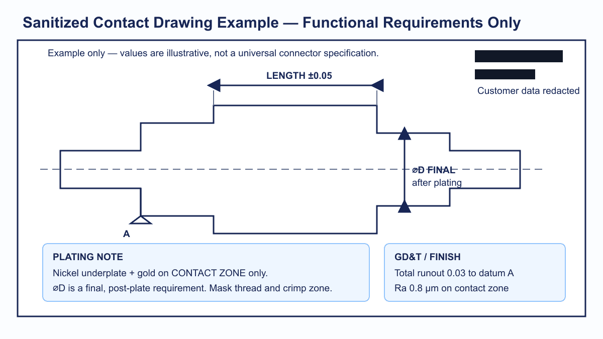
A drawing should not leave the supplier guessing whether a critical mating diameter is inspected before or after plating.
Three common approaches are useful.
| Drawing strategy | Appropriate application | Main consideration |
|---|---|---|
| Final dimensions after plating | Critical mating and retention features | Machining and plating allowances must be coordinated |
| Controlled pre- and post-plating dimensions | Features requiring inspection at both stages | Avoid conflicting independent tolerance requirements |
| Defined selective-plating zones | Different functional surface treatments | Boundaries, masking, and inspection points must be explicit |
For many precision connector contacts, defining the functional dimensions as finished dimensions after plating is a practical approach.
The manufacturer and plating supplier can then determine the process dimensions needed to meet the final specification.
Example drawing note — illustrative only:
ALL FUNCTIONAL DIMENSIONS APPLY AFTER PLATING UNLESS OTHERWISE SPECIFIED. NICKEL AND GOLD COATING REQUIREMENTS, THICKNESS LIMITS, AND SELECTIVE PLATING AREAS SHALL FOLLOW THE APPROVED PLATING SPECIFICATION. VERIFY FINAL MATING DIAMETERS AFTER PLATING.
This statement should accompany a fully defined coating specification, not replace it.
Burr Control and Surface Protection for Miniature Contacts
A burr that would be considered minor on a large machined component can be unacceptable on a miniature connector contact.
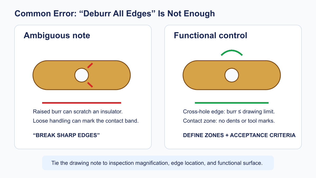
Small burrs can interfere with mating, damage insulating materials, contaminate a contact interface, or affect the quality of the plating process.
Problem locations include cross-drilled holes, slot edges, internal bore entrances, thread starts, and parting-off surfaces.
Why Generic Deburring Notes Are Often Insufficient
A drawing note such as “REMOVE ALL BURRS” provides a general instruction but does not establish the acceptable edge geometry.
For a connector pin, a large edge break near the contact tip may be just as problematic as a burr because it changes the effective mating geometry.
The drawing should identify protected functional edges and specify the permissible edge break or burr limit where needed.
For particularly sensitive features, visual inspection criteria, magnification, and approved reference samples can help avoid inconsistent acceptance decisions.
Protecting Contact Surfaces After Machining
Connector contacts can be damaged after machining through bulk handling, aggressive tumbling, contact with other metal components, or unsuitable plating fixtures.
A component that passes its dimensional inspection before plating can still become unacceptable if its mating surface is scratched or dented during subsequent handling.
For small precision contacts, separated trays, protective tubes, suitable racks, or other controlled packaging methods may be appropriate.
Handling requirements should be considered part of the manufacturing process rather than left until the shipment stage.
Inspection and Quality Control for Machined Connector Contacts
A complete inspection plan must consider both the geometry produced by CNC machining and the changes introduced during plating.
Related service: quality assurance
The appropriate measurement method depends on the feature, tolerance, accessibility, and available measurement uncertainty.
| Inspection characteristic | Possible method | Stage |
|---|---|---|
| External diameter | Micrometer, snap gauge, optical system | Pre- and post-plating as required |
| Small internal diameter | Pin gauge, air gauge, suitable optical method | As specified |
| Shoulder location | Optical measurement, CMM | Usually final inspection |
| Runout | Dial indicator with controlled datum setup | As specified |
| Surface roughness | Suitable profilometer | Before or after plating as defined |
| Residual burrs | Optical inspection | Before plating |
| Gold/nickel thickness | XRF or approved alternative | After plating |
| Surface damage | Visual or optical inspection | After plating and packaging |
| Electrical performance | Assembly-level or functional testing | As specified |
Measuring Plating Thickness
X-ray fluorescence (XRF) is widely used for measuring metallic coating thickness on suitable substrates and geometries.
ASTM B568 provides a standardized framework for X-ray spectrometric coating-thickness measurement. However, the accuracy of a measurement depends on instrument calibration, coating composition, substrate, geometry, and measurement conditions.
For miniature curved contact surfaces, the available measurement area and instrument spot size may introduce additional limitations.
Where a coating cannot be reliably measured directly on the component, the supplier may need an approved alternative method, witness samples, or destructive verification.
Witness samples are useful only when their coating results are validated as representative of the specified contact surface. The inspection arrangement should be agreed before production.
First Article Inspection and Repeat Production
First Article Inspection is particularly useful for establishing that the manufacturing process can produce the required features using the approved drawing and process route.
For connector contacts, a first-article package may include material certification, critical dimensions, geometric measurements, coating-thickness results, and visual inspection findings.
For repeat small-batch production, the manufacturer should maintain drawing revision control, inspection records, and appropriate process checks.
A part should not be accepted solely because its external dimensions pass inspection if plating, surface condition, or functional requirements remain unverified.
Example: Manufacturing a Precision Gold-Plated Connector Contact
Consider a hypothetical contact pin for an industrial electronic connector.
The component is manufactured from C14500 tellurium copper and contains a stepped mating diameter, retention shoulder, axial termination feature, and selectively plated contact zone.
The engineering team establishes the following requirements:
| Characteristic | Example specification |
|---|---|
| Material | C14500 tellurium copper, specified temper |
| Mating diameter | Ø2.000 ±0.010 mm after plating |
| Overall length | 18.00 ±0.05 mm |
| Functional shoulder | Controlled from assembly datum |
| Finish | Gold over nickel in defined mating zone |
| Surface condition | No unacceptable scratches or burrs in mating zone |
| Inspection | Critical dimensions and coating-thickness verification |
This hypothetical example illustrates a manufacturing plan; use the approved component drawing to establish acceptance limits.
The manufacturer first reviews the mating diameter and the allowable coating thickness. The calculated machining allowance is incorporated into the process plan, and the machining method is selected based on geometry and required quantity.
After turning, the component undergoes dimensional and burr inspection. Parts are then cleaned and prepared for selective plating using an approved process.
Following plating, the final mating diameter, coating thickness, surface condition, and other required characteristics are verified.
The important principle is that manufacturing acceptance is based on the finished functional contact—not merely the accuracy of the part when it leaves the CNC machine.
Common Connector Contact Manufacturing Problems
| Problem | Potential cause | Recommended action |
|---|---|---|
| Pin oversized after plating | Coating growth not accounted for | Calculate pre-plating allowance |
| Socket bore undersized | Internal plating buildup | Control coating distribution and final bore |
| Poor mating alignment | Incorrect datum or setup transfer | Review runout and positioning requirements |
| Burrs inside solder cup | Drilling or cutoff operation | Define internal burr limits and inspection |
| Scratched gold surface | Handling or packaging damage | Protect mating surfaces |
| Inconsistent contact dimensions | Tool wear or material variation | Apply process monitoring |
| Coating thickness below requirement | Plating distribution or process control | Define measurement zones and investigate |
| Unexpectedly high production cost | Excessive tolerances or complex finishing | Review functional requirements and DFM |
Many of these problems are not caused by CNC machining alone. They arise when the machining, plating, design, and inspection requirements are developed separately.
A coordinated manufacturing plan is therefore particularly important for precision connector components.
Design for Manufacturability: Before Releasing Your Contact Drawing
Before submitting a precision connector contact for quotation, engineers should verify that the drawing communicates the intended function and finished-part requirements.
- Identify the mating, retention, and termination zones.
- Specify material grade, temper, and applicable restrictions.
- Define critical diameters, fits, and functional datums.
- State whether each critical dimension applies before or after plating.
- Specify the complete coating stack and thickness limits.
- Define selective-plating areas and measurement locations.
- Identify critical burr limits and protected contact surfaces.
- Provide applicable electrical or assembly performance requirements.
- Agree on inspection reports, quantity, and packaging requirements.
Custom Connector Contact Machining at 6CNC
Precision connector contacts require more than accurate CNC turning. Material behavior, mating geometry, finishing allowances, and inspection requirements must be considered throughout the manufacturing process.
Related service: custom connector machining
6CNC supports custom CNC-machined connector components, including precision pins, terminal bodies, sockets, sleeves, and other drawing-based electrical interface parts.
Our capabilities include CNC turning, milling, and mill-turn machining, with additional finishing and inspection requirements reviewed according to the application. We work with conductive metals including copper and brass alloys, supporting prototype development and small-batch manufacturing.
For components requiring electroplating, manufacturing planning can address pre-plating dimensions, critical finished tolerances, coating requirements, and inspection arrangements before production.
Customers can submit engineering drawings and CAD models for review of component geometry, material selection, manufacturing feasibility, and quotation.
Need precision machined connector contacts?
Share your contact drawings, required material, plating specification, critical tolerances, and expected quantities with the 6CNC team.
Request a Custom Connector Machining Quote.
Frequently Asked Questions
What materials are commonly used for CNC-machined electrical connector contacts?
C11000 copper, C14500 tellurium copper, and selected brass alloys are common candidates. The selection depends on electrical conductivity, machining characteristics, strength, joining requirements, and regulatory constraints. Spring contacts may require other alloys.
How accurate can CNC-machined connector pins be?
Selected small turned features may achieve tolerances such as ±0.02 mm or ±0.01 mm under suitable conditions. Tighter requirements need component-specific manufacturing and inspection review.
How much does gold plating increase a connector pin’s diameter?
For a uniformly plated pin, the theoretical diameter increase equals twice the combined coating thickness on one surface. A 2 μm nickel layer plus a 1 μm gold layer adds approximately 6 μm to the diameter.
Should connector contact dimensions be specified before or after plating?
Functional mating dimensions are often specified after plating so the drawing directly controls the finished interface. The drawing must clearly identify which dimensions apply at each manufacturing stage.
Is C14500 better than C11000 for connector contacts?
C14500 generally offers better machinability, while C11000 offers higher conductivity. Neither alloy is universally superior. The correct selection depends on the electrical requirements, part geometry, joining method, and manufacturing process.
Is gold plating always necessary for electrical contacts?
No. Gold, silver, tin, and other finishes can be appropriate depending on the contact design, environmental conditions, mating cycles, electrical requirements, and applicable standards.
How is gold plating thickness measured?
XRF is a common method for suitable connector geometries. Other techniques may be used when component size, surface curvature, coating structure, or inspection requirements make direct XRF measurement unsuitable.